Technologies
Products
About D
2
S
News
Community
Videos
Join D
2
S
Contact Us
Menu
Videos
Technologies
Uniformity
The critical success factor
Mask Uniformity
Path to wafer uniformity
Wafer Uniformity
Achieving the best process window
GPU Acceleration
Practical full-reticle processing
Curvilinear
Better mask and wafer quality
Pixel Domain
Shape-agnostic computing
Products
PLDC
MPC for uniformity and linearity
TrueMask
®
ILT
Full-chip, Entirely Manufacturable™ ILT
TrueModel
®
Physical model for masks and wafers
CDP
GPU-accelerated design platform
About D
2
S
About D
2
S
Timeline of D
2
S Technology Highlights
Technologies
Uniformity
The critical success factor
Mask Uniformity
Path to wafer uniformity
Wafer Uniformity
Achieving the best process window
GPU Acceleration
Practical full-reticle processing
Curvilinear
Better mask and wafer quality
Pixel Domain
Shape-agnostic computing
Products
PLDC
MPC for uniformity and linearity
TrueMask
®
ILT
Full-chip, Entirely Manufacturable™ ILT
TrueModel
®
Physical model for masks and wafers
CDP
GPU-accelerated design platform
About D
2
S
About D
2
S
Timeline of D
2
S Technology Highlights
Information
News
Community
Videos
Join D
2
S
Contact Us
Menu
Page 5
Tuesday, January 10, 2023
Abhishek Shendre of D
2
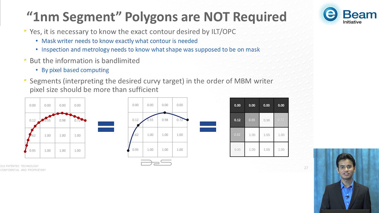
S presents the Best Paper awarded at SPIE Photomask 2022.
English
Tuesday, December 13, 2022
Semiconductor Engineering: Increased Photomask Density And Its Impact On EDA
English
Tuesday, November 1, 2022
Aki Fujimura, CEO of D
2
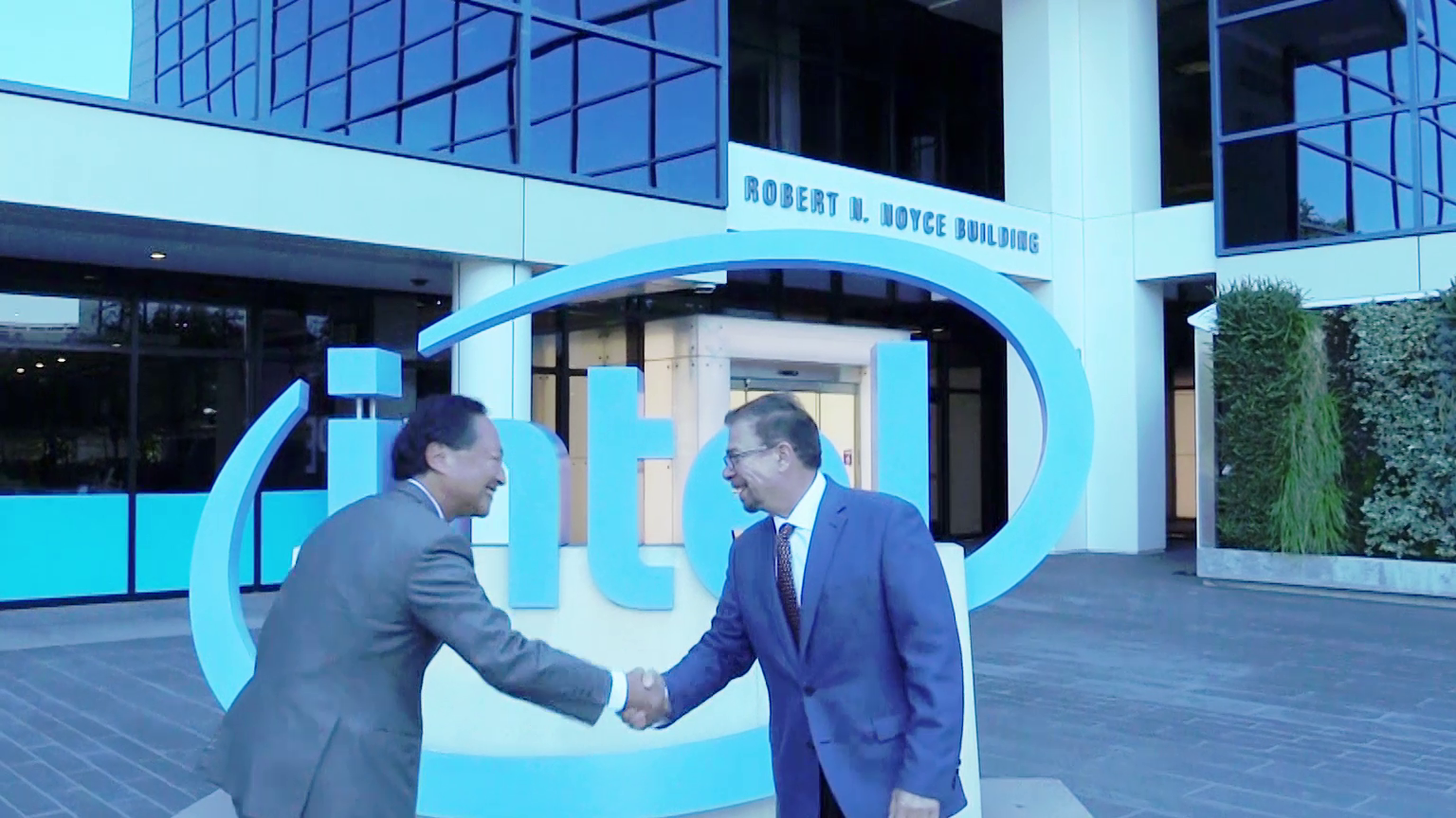
S, meets with Dr. Frank Abboud of Intel to reflect on key moments from his career.
English
Thursday, October 20, 2022
Semiconductor Engineering: Why Changes in Computing are Driving Changes in Photomasks
English
Friday, August 5, 2022
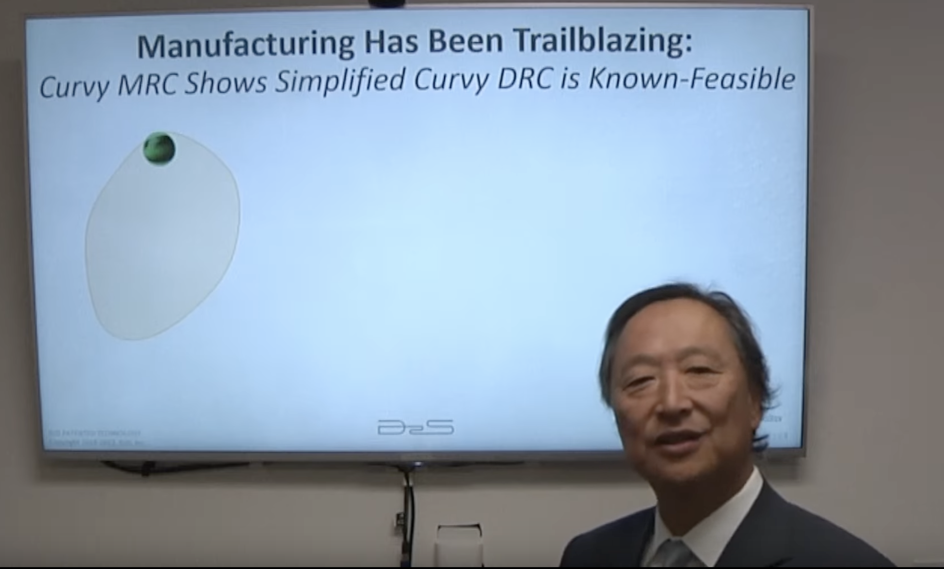
Design Automation Conference 2022 TechTalk: Is Curvy Design an Opportunity or a Dream?
English
Tuesday, April 26, 2022
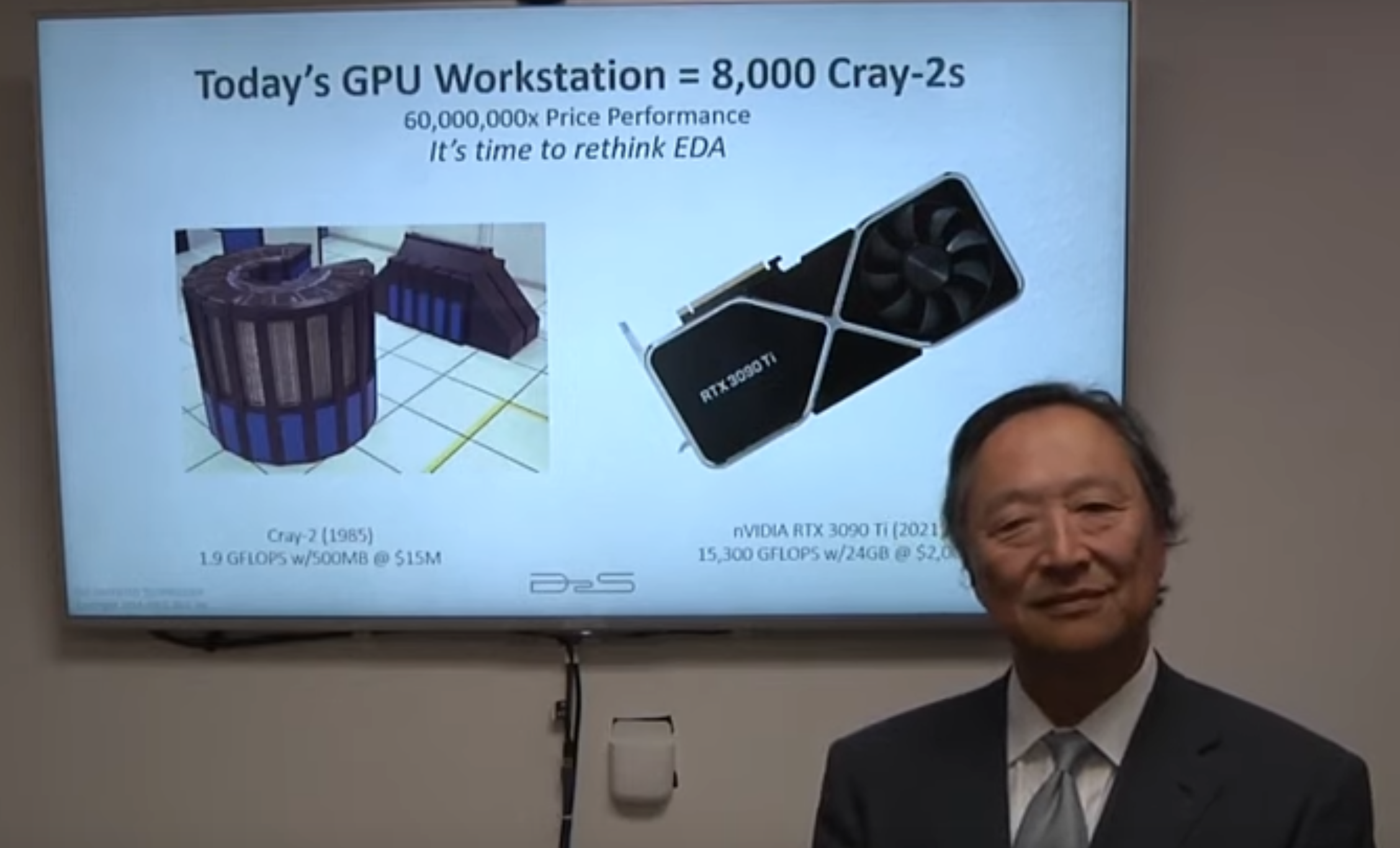
Semiconductor Engineering: Using GPUs In Semiconductor Manufacturing
English
Older Videos
Newer Videos